Challenges of Pick‑and‑Place of Silicon Die from UV-Dicing Tape
In semiconductor back-end manufacturing, diced silicon die are commonly held on UV-curable dicing tape during singulation and then removed one-by-one during die pickup. In this process flow, the wafer is laminated to dicing tape, diced, exposed to UV to reduce adhesive strength, and then the individual chips are picked for die attach or further assembly.
As semiconductor devices move toward thinner form factors and more complex packaging architectures, pick-and-place processes must adapt to the mechanical and physical challenges of ultra-thin silicon die. Successful handling requires careful control of mechanical stress, optimized tool design, advanced motion control, and integration with upstream wafer processing.
Developing reliable solutions for ultra-thin die handling is therefore a key enabling technology for the next generation of semiconductor packaging.
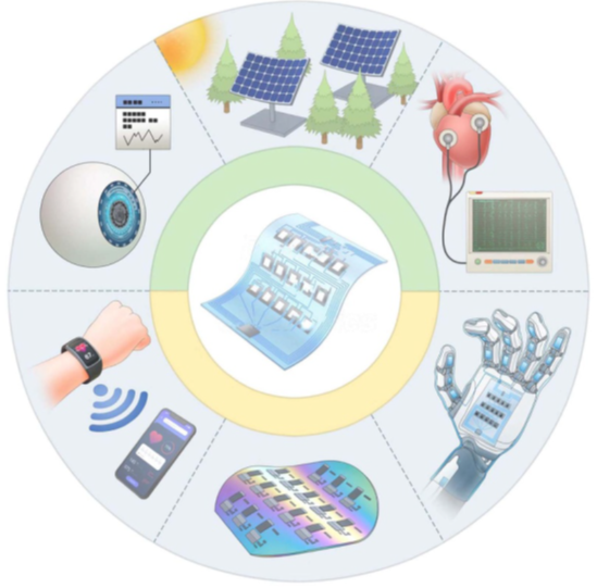
Ju Young Lee, et. al., Int. J. Extrem. Manuf. 6 (2024) 042005.
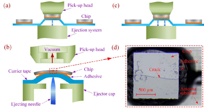
Schematic diagrams of a die that is peeled from the wafer adhesive tape (a) with a single ejecting needle and (c) with multi-needle ejector, respectively. (b) Die is bent due to the flexibility of the thin/ultrathin die, until (d) it cracks on the backside of the chip.
Zunxu Liu, et. al., IEEE TRANSACTIONS ON COMPONENTS, PACKAGING AND MANUFACTURING TECHNOLOGY, VOL. 4, NO. 9, SEPTEMBER 2014.
Transfer of Standard Thickness Die
For standard die thicknesses, pickup from UV tape is already a precision process, but the die still retains enough stiffness to behave largely as a rigid body during separation.
A key source of stress during pickup is the use of ejector pins or localized support beneath the tape. These mechanisms help initiate separation between the die and the adhesive surface, but for ultra-thin die they can also create highly localized loading. The figure shows how ejector-pin-assisted release can generate concentrated stress that may lead to die cracking or edge damage if displacement or force is not carefully controlled.
Transfer of Ultra Thin Die
As die thickness approaches ~30 µm, the overall process window narrows significantly. Standard die generally tolerate a wider range of UV dose, ejector pin height, vacuum force, and pickup speed. Ultra-thin die require much tighter control of each parameter to maintain yield and avoid damage.
Reliable pick-and-place of silicon die from UV-adhesion tape therefore depends on carefully balancing adhesion reduction, support conditions, vacuum pickup design, and motion control. What is a robust, high-speed process for conventional die can become a narrow-window, damage-sensitive operation for ultra-thin die.
As advanced semiconductor packaging continues to push toward thinner chips and more compact architectures, optimized pickup from UV dicing tape becomes a critical enabler of yield, reliability, and manufacturability.
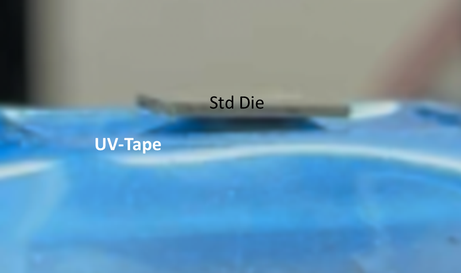
UV-Tape delamination off a standard thickness die placed on a single die VAPS. No ejector or needle is used.
TWO Problem Areas
- Inability to handle UTD: Standard vacuum-needle combination for die detachment from dicing adhesive tape is no longer suitable for UTD due to high risk for induced die cracking.
- Lack of collective handling (transfer of UTD): Collective transfer provides significant productivity improvements and will enable PLP (Panel Level Packaging), in particular.
LuxNour’s Solution
LuxNour introduces the concept of VAPS (Vacuum-Activated Patterned Stage) for the collective transfer of dies across the entire thickness range:
- No needle or ejector
- The die is mechanically supported during the tape release process by uniform forces provided by the Pickup Head(PUH)
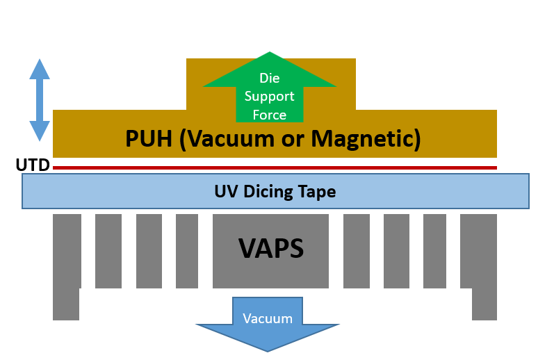
VAPS: Vacuum-Activated Patterned Stage
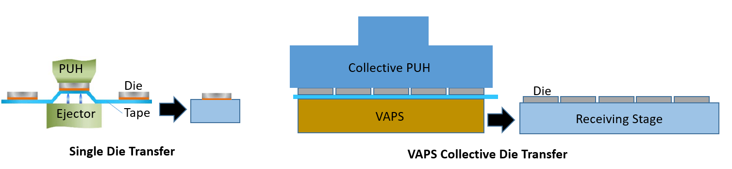
VAPS Transfer Process
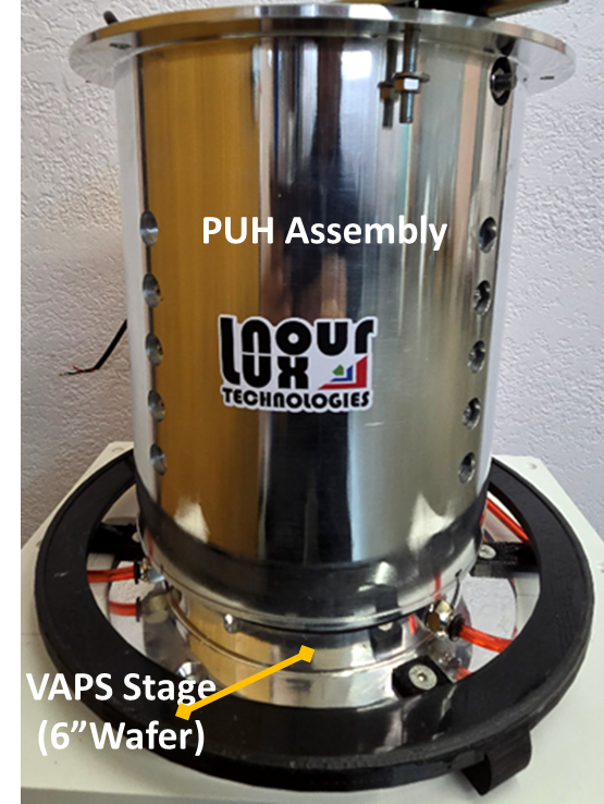
VAPS System Prototype For 6” Wafer
First VAPS prototype for the collective transfer of dies from 6” wafer.